News
Advancements and Comparative Analyses in AC to DC Power Conversion Technologies
Click: 927 Date: 01/08/2024 2::05::18 PM
Advancements and Comparative Analyses in AC to DC Power Conversion Technologies
Switching Regulators: Enhancing Efficiency in AC to DC Conversion
Switching regulators, as opposed to linear regulators, are a cornerstone of modern AC to DC power conversion, offering substantial efficiency gains. Switching regulators operate by rapidly turning the power flow on and off, controlling the energy provided to the output through the duty cycle of a pulse width modulated (PWM) signal. This method drastically reduces the power loss inherent in linear regulators, where excess voltage is dissipated as heat.
The efficiency of switching regulators typically ranges from 85% to 95%, compared to the 60% to 70% efficiency of linear regulators. Switching regulators achieve this high efficiency over a broad range of input voltages and load conditions, making them ideal for applications where battery life is critical or thermal management is a concern.
Despite their efficiency, switching regulators introduce their own challenges, such as the generation of noise due to the high-frequency switching action. This noise, spanning a spectrum from tens of kilohertz to several megahertz, can interfere with sensitive electronic components if not adequately filtered. Therefore, the design of switching regulators often includes measures to suppress electromagnetic interference (EMI), such as using shielded inductors and proper PCB layout techniques.
Switching regulators come in different topologies, including buck (step-down), boost (step-up), and buck-boost configurations, allowing them to adapt to various conversion needs. For example, a buck converter reduces voltage from a higher level to a lower level, making it suitable for applications like USB power delivery, where 5V must be regulated down from a potentially higher input voltage.
In addition to their variable topologies, modern switching regulators may incorporate synchronous rectification, which replaces diodes with low-resistance MOSFETs to further enhance efficiency. This is especially useful in low-voltage applications where the voltage drop across the diode would constitute a significant efficiency loss.
Designers often use a combination of switching and linear regulators to optimize performance. For instance, a switching regulator may be employed to step down a high input voltage to an intermediate level, followed by a linear regulator that provides the final voltage regulation with low noise characteristics.
In conclusion, switching regulators represent a highly efficient solution for AC to DC conversion in modern electronics. Their ability to minimize power loss and handle various input conditions makes them a versatile choice for power supply design. However, their complexity and the need to manage switching noise require careful consideration during the design process.
Design Principles of Full-Wave Rectification for AC to DC Power Supplies
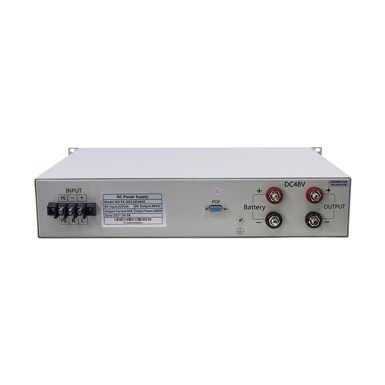
The design principles of full-wave rectification for AC to DC power supplies involve the conversion of both half-cycles of the input AC signal into a DC output. A full-wave rectifier typically uses either a center-tapped transformer with two diodes or a four-diode bridge without a center tap. The main goal is to maximize efficiency by utilizing the entire AC waveform, which is a significant advantage over half-wave rectification that uses only one half of the AC cycle.
The full-wave bridge rectifier connects the transformer secondary winding to a diode bridge that effectively routes both halves of the AC signal to produce a unidirectional flow through the load. During the positive half-cycle of the AC input, two diodes become forward-biased and allow current to pass, while during the negative half-cycle, the other two diodes conduct, maintaining the direction of current through the load. This results in a higher output voltage and better transformer utilization compared to half-wave rectification.
The peak inverse voltage (PIV) of a full-wave bridge rectifier is an important parameter, representing the maximum voltage that the non-conducting diodes must withstand. In an ideal scenario with perfect diodes, the PIV equals the maximum voltage of the transformer's secondary winding.
To smooth out the pulsating DC output and reduce ripple, a capacitor or inductor filter may be added to the circuit. The capacitor charges up when the output voltage peaks and discharges through the load when the voltage falls, providing a more constant DC level. The ripple factor, which is the ratio of the AC component to the DC component in the output, is significantly lower in a full-wave rectifier compared to a half-wave rectifier.
In summary, the design principles of full-wave rectification for AC to DC power supplies focus on:
Efficiently converting the entire AC waveform to DC.
Utilizing a center-tapped transformer or a diode bridge configuration.
Managing the PIV across diodes.
Smoothing the output using filtering components to reduce ripple.
Ensuring the rectifier can handle the desired load and power requirements.
These principles ensure that the full-wave rectifier operates effectively, providing a more consistent DC output suitable for various power supply applications.
The Impact of Capacitor Filters on the Ripple Reduction in DC Output
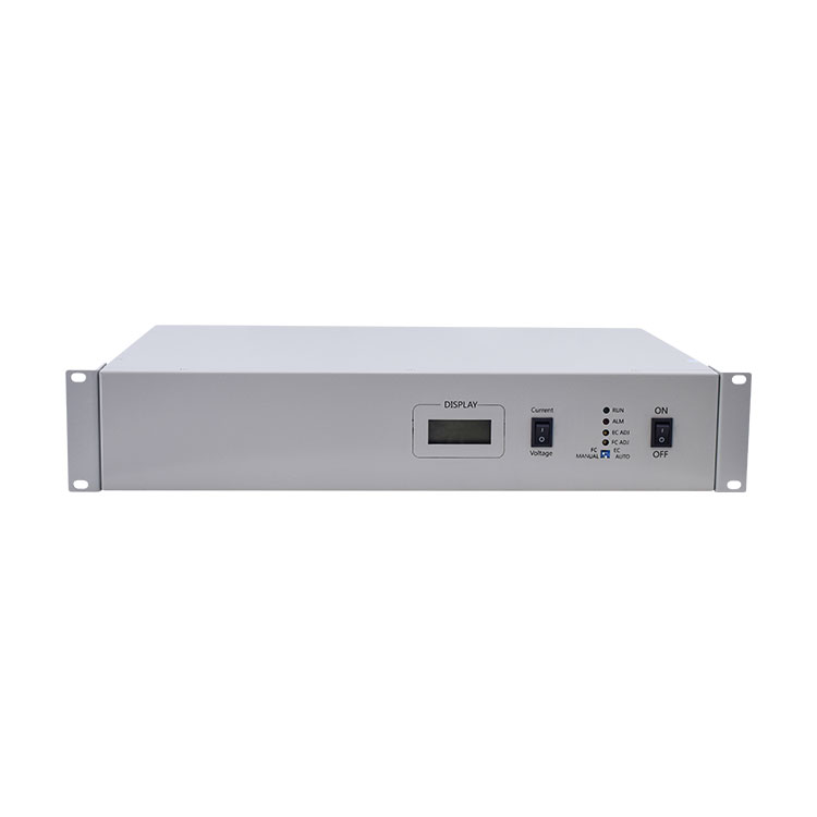
Capacitor filters play a significant role in reducing ripple in the DC output of power conversion systems. They do so by smoothing out the fluctuations in voltage that occur after AC to DC conversion. The presence of AC components within the converted DC voltage, known as ripple, can have detrimental effects on electronic circuits, potentially causing noise, heat, and reduced efficiency.
The effectiveness of a capacitor in ripple reduction is linked to its capacitance value; a larger capacitance results in a smaller ripple voltage. This is because the capacitor charges during the peaks of the AC waveform and discharges during the troughs, acting as a reservoir of electrical charge and thus leveling out the voltage variations.
In high-frequency applications, such as in switch-mode power supplies, the ripple frequency is higher, and the design may incorporate additional filtering elements like inductors to form a low-pass filter which further attenuates the ripple. Moreover, the placement of the capacitor, as close as possible to the point of load, helps in minimizing the ripple observed at the load.
It's also important to note that while increasing the capacitance can reduce ripple, it can also introduce other issues such as increased size of the power supply and longer charging times, which could affect the transient response. Therefore, designers often balance the capacitance value with these other considerations to achieve an optimal design that minimizes ripple while maintaining desired performance characteristics.
Synchronous Rectification: A Method to Improve Power Conversion Efficiency
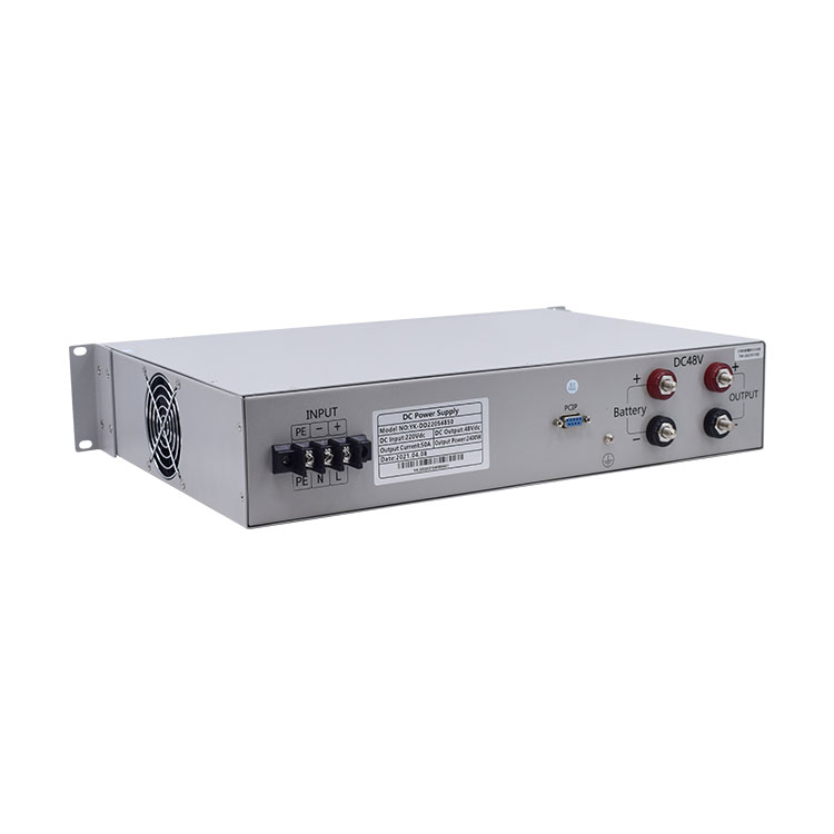
Synchronous rectification is a power conversion technique that replaces traditional diodes with low-resistance Metal-Oxide-Semiconductor Field-Effect Transistors (MOSFETs) to improve efficiency by reducing power losses. This method is synchronized with the power supply's switching frequency, ensuring that the MOSFETs conduct during the appropriate intervals, minimizing energy loss that would otherwise occur due to the forward voltage drop inherent in diodes.
The primary benefits of synchronous rectification include:
Enhanced Efficiency: The low on-state resistance of MOSFETs in synchronous rectifiers reduces conduction losses, leading to more efficient power conversion compared to diode-based rectifiers.
Lower Heat Production: With decreased power losses, synchronous rectifiers generate less heat, which is beneficial for thermal management and increases the reliability of the electronic system.
Compact Design: The use of MOSFETs in synchronous rectifiers allows for a reduced component size, enabling further miniaturization of power supplies and electronic devices.
Versatility: These rectifiers are effective over a wide range of input voltages and output currents, making them suitable for diverse applications, from telecommunications and computing to automotive and consumer electronics.
Designing synchronous rectifiers involves considerations like control methods, managing dead time to prevent cross-conduction, minimizing parasitic inductance effects, and selecting the right MOSFET for optimal performance.
The challenges faced in synchronous rectification include the complexity of control circuits and potential switching losses, particularly at higher frequencies. To overcome these and further enhance the performance of synchronous rectifiers, advancements are being made, such as using wide-bandgap semiconductors like gallium nitride (GaN) and silicon carbide (SiC) for their lower resistance and faster switching capabilities, and integrated synchronous rectifier solutions that combine control circuitry with MOSFETs into a single package.
Linear vs. Switch Mode Power Supply: A Comparative Analysis of AC to DC Conversion
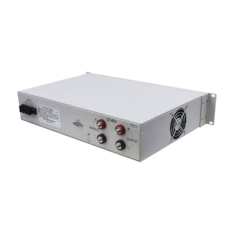
In the comparison between linear and switch mode power supplies, the key distinction lies in their method of converting AC voltage to DC voltage. Linear power supplies use a transformer to reduce the input voltage to a desired level, followed by filtration to remove any residual AC currents. This process typically results in low output ripple and noise, beneficial for sensitive applications like audio equipment or precision measurement tools. However, linear power supplies are less efficient, as they dissipate excess energy as heat, leading to larger and heavier designs.
Switch mode power supplies, on the other hand, employ high-frequency switching techniques to convert the input voltage. They rapidly switch the input voltage on and off, controlling the energy provided to the transformer and subsequently to the load. This method is much more efficient, resulting in less energy wasted as heat and allowing for smaller, lighter power supplies. However, the high-frequency switching can introduce more electrical noise (ripple) into the output, which may be problematic for certain applications.
The choice between linear and switch mode power supplies ultimately depends on the specific requirements of the application. Linear power supplies may be favored in low-noise, high-precision environments, whereas switch mode power supplies are typically chosen for their efficiency, compact size, and ability to handle a broader range of input voltages. When selecting a power supply, considerations such as the ambient temperature rating, power output needs, and compliance with regulatory standards like Class 2 for power output and Devicenet for networked power and data integration should be taken into account.
In conclusion, while switch mode power supplies are generally preferred for their efficiency and compact size, linear power supplies are still relevant for applications demanding minimal noise and high precision. Advances in technology continue to refine both types of power supplies, making them more efficient and adaptable to a variety of uses.
